Carultch
Senior Member
- Location
- Massachusetts
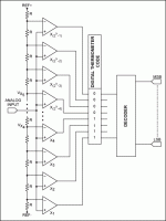
I'm working with this product, and I'm trying to make sense of how to wire the following pins:
Pin 6: Write/Ready, with an overbar on "write"
Pin 7: Mode select
Pin 8: Read, with overbar
Pin 9: Interrupt, with overbar
Pin 13: Chip select, with overbar
Pin 18: Overflow, with overbar
The datasheet just shows these wired to a microprocessor, but it doesn't show what signals the microprocessor is expected to send for each application. In my application, I'd like the ADC to stand on its own and not need any supplimentary signals from a microprocessor. Either in real-time, or close enough to real time (e.g. every 100 microseconds or similar order of magnitude). I'm only using the single group of 8 bits for any given analog input signal. I'm open to recommendations on other ADC chips you think could work better with my goals.
Here's my guess at how it's supposed to be wired, from what I gather reading the datasheet:
Pin 6: Possible Jumper from Pin 9
Pin 7: 0V ground
Pin 8: 0V ground
Pin 9: Possible Jumper to Pin 6
Pin 11 (Vref-): to 0V ground with 100 nF capacitor in parallel (not sure if capacitor is really necessary)
Pin 12 (Vref+): to +5V with wire, and 100nF capacitor to ground
Pin 18: no connect. Will be logical high output, as long as there's no overflow