Transformer 1 and 2 are both separately derived and each would have its own N to G bond plus a GEC run from each main or system bonding jumper, common busbar, to the facility (common contiguous) grounding electrode system.
Then you describe loading 1's loads onto 2, which could be described typically as a dual source bus with a tie, and you say the majority data center loads and configured line to neutral. You would have high neutral current with two (or more) N to G bonds putting your high neutral current on the EGC and GEC paths.
If the source transformers are remotely located from the switchgear bond, it is possible or likely that also has another N to G bond, with two such source making four minimum have to be checked. There should be only one if at all possible.
This is one of the reasons, this type of data center dual source bus, would only have line to line connected loads at the dual bus, where the system bonding jumper is, because of the possibly unavoidable multiple N to G bonds. No neutral connected loads is one way to clean it up, but not possible in your case.
Anyway, you have identified where to look.
I would recommend starting at square 1. Look at what you have on paper and decide where your one main or system bonding jumper with its associated GEC conductor should be. Then examine each transformer and downstream switchgear for their present or not N to G points. Survey knowing what you are looking for before proceeding.
Did not read the entire thread.
This morning I was able to verify my assumption.
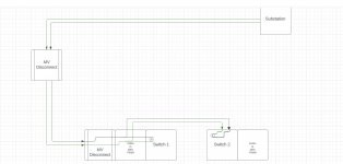
So even though we’re not using switch 1 to service any load, it’s still hooked up, and the G+N are bonded. The same bus bars then go over to switch 2 from the transformer and in that switch also has G+N bonded.
What I believe is happening is we have a parallel path in the same SDS.
The following drawing is now verified as accurate and this more than likely explains what we’re seeing.

