Single Phase current draw for a 3 phase output VFD: technical discussion

Status
Not open for further replies.
No, you are not misunderstanding. And you bring up a valid point.

1) A power factor being exhibited on the motor conductors is imminent.
2) Recommended-for-VFD motors have improved power factor characteristics,
3) but not so much that we can totally disregard it. :happyno:

Anyway, that's why I preferred to state the relationship as Pi>Po... as it takes power factor out of the equation.

4) Ii/Io > 1.732 is simply a generalization with power factor correction built in.
5) We've already heard that conversion losses raise the 1.732 factor.
6) Well, motor power factor lowers the elusive factor.

Not sure why you wrote anything in this post.

1) Please explain what is "about to happen?"
2) Nonsense!
3) Who has ever considered PF when applying a VFD?
4) Nonsense again! 1.732 has never had a thing in common with PF and never will.
5) Some folks suggested that; it has not been proven as fact.
6) What is "an elusive factor?" II call BS on this too.
 
170521-1714 EDT

Something I have not previously mentioned is that because of inductance in series with each diode there are short times at the transition points where the turning off diode remains on slightly longer.
Care to estimate the time or scope it?
 
re: a few nanoseconds of junction reverse recovery

Notice I did say there was a dc link capacitor (in every VFD I've ever seen the schematic of except some experimental matrix converters) Since you so badly want to see a case where you can say "see, I told you more than 2 diodes conduct" here is one you can say you were correct in some cases -- no load, no link cap, :?

Just junction reverse recovery currents, a few microamps in every diode all the time.

diodereverserecoverynoloads.jpg
 
Increase the load and/or decrease the capacitance until you only get one hump per cycle per diode, such as the graph posted by gar (actually I'm assuming that's one hump per cycle in his image).

And this one, no DC link capacitor, 25 A load, so you can say " see, there is a 30 us period when there are 3 diodes conducting". This is called the reverse recovery time of the diode. This is for a slow didoe, there are 'fast' and 'ultra fast', and FRED, etc. diodes where this time is in the 10s of nanoseconds.
If ya want to get into foundry fabrication of different diodes, junction capacitance, charge mobility, etc. , start a new thread.

Goodnight :bye:

no cap.jpg
 
And this one, no DC link capacitor, 25 A load, so you can say " see, there is a 30 us period when there are 3 diodes conducting". This is called the reverse recovery time of the diode. This is for a slow didoe, there are 'fast' and 'ultra fast', and FRED, etc. diodes where this time is in the 10s of nanoseconds.
If ya want to get into foundry fabrication of different diodes, junction capacitance, charge mobility, etc. , start a new thread.

Goodnight :bye:

View attachment 17605
Interesting. I was curious as to what that time would be. Thanks.
 
170521-1928 EDT

Smart $:

In your post numbered #119 the plot of mine that you showed is for the diode output current into a very large capacitor, 53,000 ufd with a shunt load of 5 ohms. Time constant about 0.25 seconds, pulsed every 8.3 mS. Output voltage ripple moderately low.

The source of voltage excitation is a center tapped transformer with a full wave rectifier output. Means two diodes with only one conducting at a time. This could be called a two phase 1/2 wave rectifier.

The conduction of one diode and its current is pretty much the same for any one diode feeding a capacitor input filter independent of the number of phases.

.
Like this, only with a capacitor...?

3.jpg


As depicted, a diode will conduct up to just under 180° of a cycle as bias voltage shortens the "hump". Put a 3Ø source in the scenario above. The humps will be 120° apart, which means they would overlap by nearly 60° (30° to each side).
 
Interesting. I was curious as to what that time would be. Thanks.

If you are interested, those waveforms were generated on the 'student' version of Orcad PSpice.

You can download a FREE program at:

http://www.orcad.com/products/orcad-lite-overview?gclid=CN3A1PKagtQCFVFsfgodVIYGlg

The learning curve for that program is not too difficult (easy for me to say, have been using it since 1986 or so.

Attached is the simple 3 phase circuit I put in a previous post.
hmm, site will not let me attach the .opj file, will try to e-mail it to you.
 
Not sure why you wrote anything in this post.

1) Please explain what is "about to happen?"
2) Nonsense!
3) Who has ever considered PF when applying a VFD?
4) Nonsense again! 1.732 has never had a thing in common with PF and never will.
5) Some folks suggested that; it has not been proven as fact.
6) What is "an elusive factor?" II call BS on this too.
Not that I want to dismiss your points, but I believe you are taking my statements out of their discussion context.

You are also pushing the boundaries of friendly, constructive criticism. For example, my use of the word imminent was meant as likely to be the case... not like "Danger is lurking around the corner and I'm headed there now!" Perhaps I used it in the wrong vain, but your call to rebuke slang use of the term is enough for me to just totally disregard your reply... moving forward.
 
170521-2037 EDT

mivey:

In response to your post #122.

See section 1-6. Overlapping Currents Caused by Transformer Reactances on P-19 of "Theory and Application of Industrial Electronics", Gage and Bashe, McGraw-Hill, 1951.

From Google there are about 235 libraries with this book. Google Books only shows a snippet from the page, copyright.

.
 
170521-2104 EDT

Smart $:

Yes to your post #127.

It is interesting to observe that as the number of equally spaced phases increases that ripple greatly diminishes, and average DC voltage approaches peak AC voltage. Thus, with many phases for an industrial application little or no capacitive filtering may be needed.

.
 
170521-2037 EDT

mivey:

In response to your post #122.

See section 1-6. Overlapping Currents Caused by Transformer Reactances on P-19 of "Theory and Application of Industrial Electronics", Gage and Bashe, McGraw-Hill, 1951.

From Google there are about 235 libraries with this book. Google Books only shows a snippet from the page, copyright.

.
I guess you could adopt the 10% dc voltage drop mentioned to contrive a model then calculate the overlap but I'm not going to. I was not thinking of a counter emf due to the source transformer but more of an internal component delay. Very interesting read though.
 
If you are interested, those waveforms were generated on the 'student' version of Orcad PSpice.

You can download a FREE program at:

http://www.orcad.com/products/orcad-lite-overview?gclid=CN3A1PKagtQCFVFsfgodVIYGlg

The learning curve for that program is not too difficult (easy for me to say, have been using it since 1986 or so.

Attached is the simple 3 phase circuit I put in a previous post.
hmm, site will not let me attach the .opj file, will try to e-mail it to you.
Thanks. It has been a while since I used PSpice so any modern versions would have to be easier. Not sure I'm up for it though.
 
Increase the load and/or decrease the capacitance until you only get one hump per cycle per diode, such as the graph posted by gar (actually I'm assuming that's one hump per cycle in his image).
Let me try yet again.
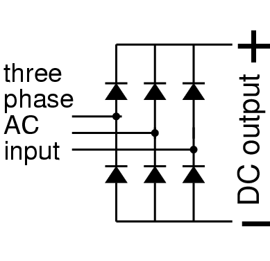
Look at the three phase waveform I posted. Unless you doubt the validity of that, you can clearly see that red is more positive that either of the other two phases for 120 degrees. That means that the diodes in the top half of the bridge on those other two phases are reverse biased for that 120 deg period thus won't conduct. That's their function/characteristics. It's the same for the other two phases. Each has a 120deg out of 360 deg window to the exclusion of the other two. So, only one can conduct for that period. It may conduct for all or part of that period. Neither of the others can.

One diode at a time in the top half. Same in the bottom half. So only ever two devices concurrently.

tridge.png
 
And this one, no DC link capacitor, 25 A load, so you can say " see, there is a 30 us period when there are 3 diodes conducting". This is called the reverse recovery time of the diode. This is for a slow didoe, there are 'fast' and 'ultra fast', and FRED, etc. diodes where this time is in the 10s of nanoseconds.
If ya want to get into foundry fabrication of different diodes, junction capacitance, charge mobility, etc. , start a new thread.
Well said that man.
Overlap angles have, in my experience, some relevance in high current low voltage applications but not in this discussion.
 
Let me try yet again.
Look at the three phase waveform I posted. Unless you doubt the validity of that, you can clearly see that red is more positive that either of the other two phases for 120 degrees. That means that the diodes in the top half of the bridge on those other two phases are reverse biased for that 120 deg period thus won't conduct. That's their function/characteristics. It's the same for the other two phases. Each has a 120deg out of 360 deg window to the exclusion of the other two. So, only one can conduct for that period. It may conduct for all or part of that period. Neither of the others can.

One diode at a time in the top half. Same in the bottom half. So only ever two devices concurrently.

tridge.png
But those voltages are shown with neutral as a reference and the neutral is not even in the scheme of things.

Line to line voltage is what matters. Each two have a common line. For example AB and AC. Let's plot them...

AB_AC_voltage_plot.png


As you can see, A is positive with respect to B over a range of 180°. A is positive with respect to C over a range of 180°. The 120° you refer to is depicted between 300° and 420° in my diagram. If there is only a resistive load connected, what diodes are conducting and when during this 120° period?
 
170521-2467 EDT

Smart $:

In Bes's drawing label the top AC line R, the middle G, and the bottom B.

In Bes's plot of three sine waves consider R and B and see that they have a common reference point of G. At 30 degrees on the plot B is -1 (negative peak), and R is a +0.5 (sine of 30 deg). The difference is 1.5 . The R top diode is on, and the bottom B diode is on. The top B and G diodes are off

At 30 degrees the B and G top diodes are reversed biased because B is negative, and G is less positive than R.

At 60 degrees R and B magnitudes are 0.866 and thus the difference is 1.732, and top B and G remain back biased.

The voltage between R and B is larger than R and G until B and G intersect at 90. Thus, the bottom G diode remains reversed biased until this point.

At 90 degrees conduction of top R diode shifts from bottom B to bottom G.

This same analysis can be continued thru the remainder of the cycle.

It is late and I have only limitedly checked what I wrote.

.

Fair enough.
But there is no G if you mean ground.
Forgive me if I have misinterprated what you meant.
 
Fair enough.
But there is no G if you mean ground.
Forgive me if I have misinterprated what you meant.

Labels R as in Red, B as in Blue and G as in Green.
No reference to "ground" except perhaps implied in the fact that the three AC lines are the voltages with respect to some common fixed point.

And when the voltages plotted are line to line voltages, even that implicit reference is gone.
 
Last edited:
Status
Not open for further replies.
Top